Categories
Recent Posts
In the world of power electronics, efficiency and versatility are paramount. Whether you're designing a portable device that needs to squeeze every last drop of energy from a battery, or an industrial system that must handle fluctuating input voltages, the buck-boost power supply stands as one of the most indispensable tools in an engineer's arsenal. This isn't just another theoretical tutorial—this is a comprehensive walkthrough that combines power electronics fundamentals with professional-grade PCB design principles to help you create a robust, high-performance buck-boost converter from scratch.
Understanding the Buck-Boost Topology: Why It's Essential
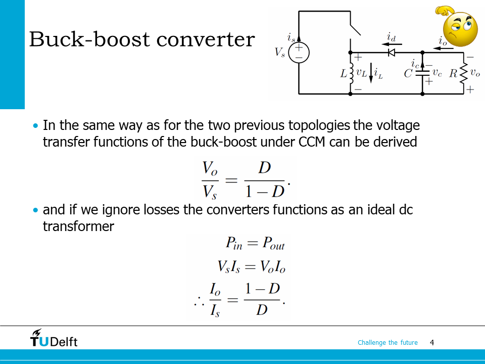
The fundamental principle behind buck-boost operation is elegantly simple yet mathematically sophisticated. When the main switch (typically a MOSFET) turns on, current flows through the inductor, storing energy in its magnetic field while the diode is reverse-biased and the output capacitor supplies the load. When the switch turns off, the inductor's collapsing magnetic field generates a voltage that forward-biases the diode, allowing current to flow to the output. The voltage transformation ratio follows the relationship Vout/Vin = D/(1-D), where D represents the duty cycle of the switching signal.
Modern implementations have largely replaced the traditional asynchronous design (with a diode) with synchronous buck-boost architectures using a second MOSFET instead of the diode. This substitution dramatically improves efficiency by eliminating the 0.3-0.7V forward voltage drop across the diode, particularly crucial for low-voltage applications where every millivolt counts.
Component Selection: The Foundation of Performance
Creating an exceptional buck-boost power supply begins with thoughtful component selection. Your choices here will ripple through every aspect of performance—efficiency, thermal characteristics, electromagnetic compatibility, and long-term reliability.
The Inductor: Your Energy Storage Workhorse
The inductor represents the heart of any switching converter, and buck-boost designs place unique demands on this component. Unlike buck converters where inductor current flows continuously to the output during both switching phases, buck-boost inductors see all output current delivered only during the off-time. This results in higher peak currents and greater current ripple for equivalent power levels.
When selecting an inductor, target an inductance value that yields approximately 20-40% current ripple relative to the average inductor current. This sweet spot balances core losses against conduction losses while maintaining good transient response. The saturation current rating must exceed your maximum expected peak current by at least 20-30%—saturation causes inductance to collapse catastrophically, leading to current spikes that can destroy semiconductors.
Shielded or semi-shielded inductors deserve serious consideration for buck-boost applications. The magnetic field fringing from unshielded inductors can couple noise into sensitive analog circuitry or induce eddy currents in nearby copper planes, degrading performance. For high-current designs, consider composite core materials or powdered iron cores that offer soft saturation characteristics rather than ferrite's abrupt saturation behavior.
Power MOSFETs: Minimizing Losses
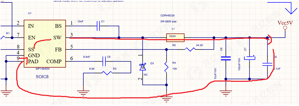
The main switching transistors in your buck-boost converter face demanding electrical stress. They must withstand the sum of input and output voltages during switching transitions, exhibit low on-resistance to minimize conduction losses, and switch rapidly to reduce transition losses. For the high-side switch in synchronous designs, pay particular attention to gate charge specifications—lower Qg values reduce gate drive losses and enable faster switching.
Dual-channel MOSFETs in a single package offer compelling advantages for compact buck-boost designs. They ensure thermal and electrical matching between switches while simplifying layout. Always consult the Safe Operating Area (SOA) curves, remembering that buck-boost converters see higher current stress than equivalent-power buck converters due to the topology's current multiplication effect.
Control IC: The Brain Behind the Operation
Modern buck-boost controllers integrate sophisticated features that simplify design while enhancing performance. Look for controllers offering:
Advanced controllers implement hysteretic current-mode control or constant on-time control architectures that offer superior transient response compared to traditional voltage-mode control. For battery-powered applications, controllers with PFM/PWM mode switching automatically transition to pulse-frequency modulation at light loads to maintain efficiency, a critical feature for extending battery life.
PCB Layout: Where Theory Meets Reality
Here's where your design transitions from simulation to physical hardware—and where many theoretically sound designs falter. Buck-boost PCB layouts present unique challenges because high currents flow through shared nodes that see rapid voltage transitions. Poor layout practices manifest as excessive noise, poor regulation, EMI failures, and inexplicable instability.
Strategic Component Placement
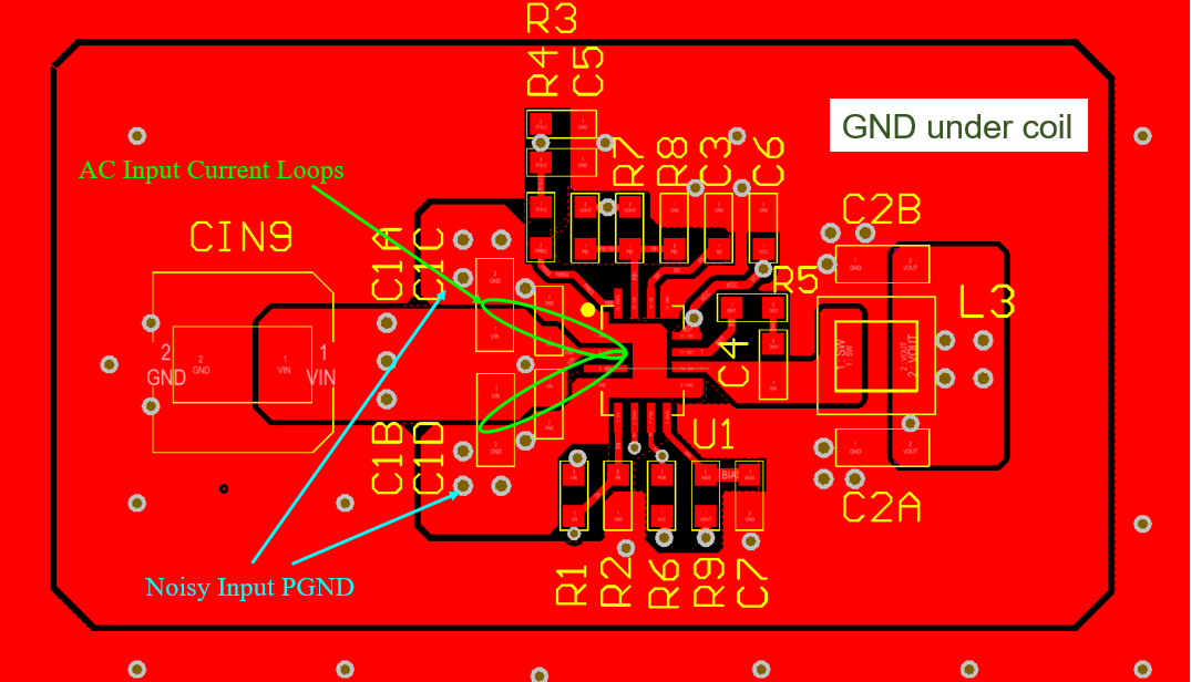
Begin your layout by positioning the power stage components—the inductor, input capacitors, output capacitors, and switching transistors—in the tightest possible grouping. The goal is to minimize loop areas for high di/dt current paths, which are the primary sources of magnetic field radiation.
Place input ceramic capacitors immediately adjacent to the high-side switch drain (for the input loop) and the low-side switch source. These capacitors supply the transient current demands during switching transitions; every millimeter of additional trace length introduces parasitic inductance that degrades performance and generates noise.
The inductor should sit close to both switches, with the switch node connection kept as compact as possible. This node experiences voltage swings equal to the sum of input and output voltages with extremely fast edge rates—it's a potent noise source that must be contained. Consider using a shielded inductor or orienting the inductor such that its magnetic field couples minimally with sensitive circuitry.
Critical Current Loops: Your EMI Enemies
Two current loops demand obsessive attention in buck-boost layouts:
Both loops must be minimized in area and implemented with wide, short traces on a solid ground plane. Use multiple vias liberally when transitioning between layers—never rely on a single via to carry switching current. A good rule of thumb is one via per ampere of DC current, plus additional vias for AC current sharing.
The Switch Node: Handle With Care
The switch node—where the inductor, both switches, and the bootstrap capacitor connect—presents the most challenging layout constraint. This node swings rapidly between ground and the input voltage plus output voltage, creating capacitive coupling to adjacent traces and electric field radiation.
Keep the switch node copper area minimal—just enough to handle current with acceptable temperature rise. Resist the temptation to create large copper pours "for better current handling" on this node; the increased parasitic capacitance couples switching noise everywhere. Maintain adequate clearance (typically 0.5-1mm for low-voltage designs, more for higher voltages) from the switch node to sensitive analog signals, feedback networks, and compensation components.
Implement a grounded copper pour on adjacent layers beneath the switch node to provide electric field termination, but ensure this ground is well-connected to your main ground plane to prevent ground bounce.
The voltage feedback divider and error amplifier compensation network determine your converter's stability and transient response. These high-impedance nodes are exquisitely sensitive to noise pickup and must be protected from the aggressive electromagnetic environment of the power stage.
Route feedback traces as differential pairs if your controller supports remote sensing, or as a single trace from the output voltage sense point (located at the output capacitor, not the inductor or switch node) to the controller. Keep these traces short and away from the inductor, switch node, and gate drive traces. Place the feedback divider resistors and compensation components immediately adjacent to the controller IC to minimize noise pickup on these high-impedance nodes.
Implement a Kelvin connection for current sensing if your controller supports it—this technique eliminates common-mode voltage errors by sensing current with a dedicated pair of traces that don't carry significant load current.
Thermal Management: The Silent Killer
Buck-boost converters often operate at duty cycles near 50% when Vin ≈ Vout, a condition that maximizes current stress in the switches and inductor. This creates challenging thermal scenarios where both switches share conduction losses nearly equally, unlike buck converters where one switch sees minimal duty cycle.
Utilize thermal vias beneath power components—arrays of small vias (0.3mm diameter typical) with solder mask relief to allow solder filling—connecting surface-mount power devices to internal copper planes or backside ground planes. For discrete MOSFETs, extend drain and source copper areas to maximize heat spreading while respecting switch node area constraints.
Consider thermal relief patterns for through-hole components that must solder reliably while maintaining adequate copper area for heat dissipation. The inductor often dominates thermal concerns—ensure adequate copper area beneath and around the inductor, and consider elevated current ratings if your enclosure restricts airflow.
Advanced Techniques for Professional Results
Input and Output Filtering
Buck-boost converters generate significant ripple current on both input and output terminals due to the discontinuous current nature of the topology. Implement multilayer ceramic capacitors (MLCCs) in parallel with bulk capacitors at both ports. The MLCCs handle high-frequency ripple while electrolytic or tantalum capacitors provide bulk energy storage.
Add a small LC filter or common-mode choke on the output for noise-sensitive applications. A 1-2µH inductor with a 10µF capacitor creates an effective second-stage filter with minimal additional voltage drop. Be mindful that output filters affect loop stability—account for them in your compensation design.
Synchronous Rectification Nuances
Synchronous buck-boost controllers require dead-time insertion to prevent shoot-through when both switches might briefly conduct simultaneously. Insufficient dead-time causes destructive current spikes; excessive dead-time forces current through the low-side body diode, degrading efficiency and potentially causing thermal issues.
Modern controllers automatically adjust dead-time, but verify operation across temperature extremes. The low-side MOSFET body diode conducts during dead-time intervals—ensure this diode can handle the peak inductor current and that thermal calculations account for these additional losses.
Light-Load Efficiency Optimization
Battery-powered applications spend significant time in light-load or standby conditions. Implement discontinuous conduction mode (DCM) operation or pulse-skipping modes that reduce switching losses by suspending switching cycles when the load demand is minimal. Some controllers offer frequency foldback that reduces switching frequency at light loads while maintaining regulation.
Consider input disconnect features that physically isolate the battery from the converter during shutdown, preventing quiescent current drain. This feature is particularly valuable for lithium-ion applications where even microamp-level drain currents significantly impact shelf life.
Even the most meticulous layout requires empirical validation. Your testing protocol should include:
Conclusion: Mastering the Art
Creating an exceptional buck-boost power supply transcends mere circuit theory—it demands intimate understanding of electromagnetic principles, thermal management, and manufacturing realities. The PCB is not merely a component carrier but an integral part of the circuit, with parasitic elements that dominate high-frequency performance.
By respecting the unique challenges of buck-boost topology—higher current stress, complex switching patterns, and sensitive analog nodes—you can create power supplies that deliver exceptional performance across wide operating ranges. The investment in careful component selection, strategic placement, and rigorous validation yields dividends in reliability, efficiency, and electromagnetic compatibility.
Whether you're powering a sophisticated IoT sensor node or a rugged industrial controller, the principles outlined here provide the foundation for success. Remember: in power electronics, the difference between a functional prototype and a production-ready design lies in the details—details that begin on the schematic but are ultimately realized through thoughtful PCB implementation.
Send your PCB Files or Bom List now
GET IN TOUCHTel : +86 75589230220
E-mail : Sales@ucreatepcb.com
Office Address : Room 315, Building C, Yunhai Industrial Park, Longgang District, Shenzhen
PCB Factory :Xiangshui River Industrial Zone, Daya Bay, Huizhou. / No. 11, East District, Industrial Park, Suichuan County, Jiangxi Province
SMT Factory : 3/F, Building 28, Chentian Industrial Zone, Xixiang Street, Bao'an District, Shenzhen, China